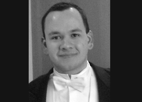
ABOUT EDGAR

After completing his A-level diploma at the Lycée Français Paul Valéry in Cali, he went to France to study Physics at the University of Paris XI. As part of his final Master’s degree project, which he did at the University of Groningen in The Netherlands, he got involved in the development and study of electronic devices made from carbon nanotubes. This strengthened his interest in and passion for the field of Nanoscience, which later brought him to the Kavli Institute of Nanoscience at Delft University of Technology in The Netherlands, where he completed his Ph.D. in Physics in the field of Molecular Electronics. Interested in the world of industry, in 2010 he left academia and joined ASML, a Dutch company which is currently the world’s main supplier of lithography systems for the semiconductor industry. Edgar worked in ASML’s research department for the Extreme Ultraviolet (EUV) lithography program, which will enable the development of better performing integrated circuits (such as DRAM/Flash memories and CPUs) in the near future. At ASML, Edgar developed skills in the fields of material science, plasmas, optics, and particle adherence, to cite just a few. Thanks to ASML’s partnership with Dutch and foreign universities, Edgar kept a foot in academia through research projects in which he participated with Ph.D. students. At present, he lives in Dresden, Germany, with his family and continues being an associate of us.